The global scanning electron microscope (SEM) market size has experienced remarkable growth in recent years, with a value of approximately USD 4.49 billion in 2023. Projections indicate a further surge in the market, with an anticipated compound annual growth rate (CAGR) of 8.30% from 2024 to 2032, aiming to reach an impressive USD 9.24 billion by 2032. This growth trajectory underscores the increasing significance of scanning electron microscopes in various fields, particularly in materials science research. In this comprehensive exploration, we delve into the multifaceted role of SEMs in materials science, encompassing their evolution, applications, advantages, challenges, recent advances, and future trends.
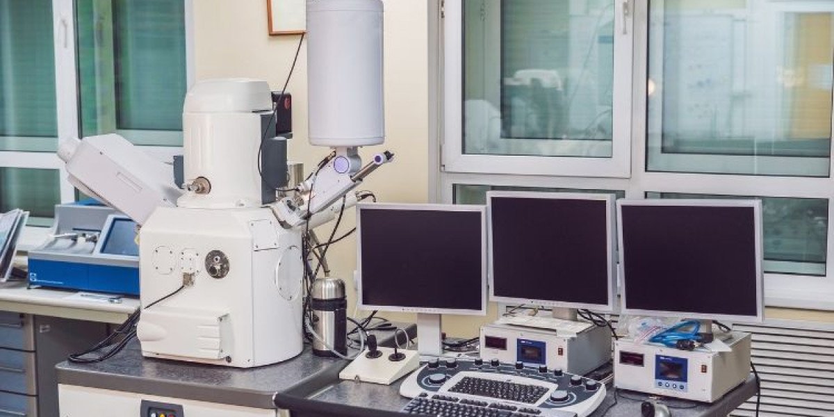
Evolution of Scanning Electron Microscopes
The journey of scanning electron microscopes began with the groundbreaking work of Ernst Ruska and Max Knoll in the early 20th century. Their invention laid the foundation for electron microscopy, revolutionizing our ability to visualize structures at the nanoscale. Over the decades, SEM technology has undergone significant advancements, driven by innovations in electron optics, vacuum systems, and detector technology.
Early SEMs were characterized by bulky designs and limited resolution capabilities. However, the development of field emission SEMs (FE-SEMs) and environmental SEMs (E-SEMs) in the latter half of the 20th century marked significant milestones in SEM evolution. FE-SEMs offered improved imaging resolution and sensitivity, enabling researchers to observe finer details of specimens. E-SEMs, on the other hand, introduced the capability to analyze specimens under controlled environmental conditions, expanding the range of applications in materials science research.
In recent years, advancements in SEM technology have led to the development of high-resolution SEMs equipped with sophisticated imaging and analytical capabilities. These modern instruments boast enhanced resolution, faster imaging speeds, and integrated energy dispersive X-ray spectroscopy (EDS) systems for elemental analysis. Furthermore, innovations such as aberration correction and cryo-SEM have pushed the boundaries of imaging capabilities, enabling researchers to explore biological specimens and delicate materials with unprecedented clarity and precision.
Applications of SEMs in Materials Science Research
SEMs play a pivotal role in materials science research by facilitating the analysis and characterization of a wide range of materials at the micro- and nanoscale levels. Their versatility and high-resolution imaging capabilities make them indispensable tools for studying various aspects of materials, including microstructure, morphology, elemental composition, and mechanical properties.
One of the primary applications of SEMs in materials science is surface imaging, which involves visualizing the topography and morphology of material surfaces. SEM images provide valuable insights into surface features such as grain boundaries, defects, and surface roughness, which are critical for understanding material properties and performance. Additionally, SEMs are utilized for phase identification and characterization, enabling researchers to distinguish between different phases within a material and analyze their distribution and morphology.
Another essential application of SEMs is elemental analysis using EDS, a technique that allows researchers to determine the elemental composition of materials based on X-ray emissions generated by electron beam interactions. EDS analysis provides valuable information about the chemical composition of materials, including the presence of impurities, alloying elements, and dopants. Elemental mapping, a variant of EDS analysis, allows researchers to visualize the spatial distribution of elements within a sample, providing insights into compositional variations and segregation phenomena.
Furthermore, SEMs are employed for the characterization of mechanical and chemical properties of materials, including hardness, elasticity, and fracture behavior. Mechanical property analysis involves techniques such as nanoindentation and electron backscatter diffraction (EBSD), which enable researchers to assess the mechanical response of materials under different loading conditions. Chemical property analysis encompasses methods such as electron energy loss spectroscopy (EELS) and wavelength-dispersive X-ray spectroscopy (WDS), which provide information about chemical bonding, electronic structure, and valence states of elements within materials.
Advantages of Using SEMs in Materials Science Research
SEMs offer numerous advantages over other microscopy techniques, making them indispensable tools for materials science research. One of the primary advantages of SEMs is their high-resolution imaging capabilities, which enable researchers to visualize fine details of materials with spatial resolutions ranging from submicron to nanometer scales. This level of resolution is essential for studying microstructural features, nanoscale phenomena, and surface morphology of materials.
Additionally, SEMs offer versatility in sample types and sizes, accommodating a wide range of materials, including metals, ceramics, polymers, composites, and biological specimens. Unlike transmission electron microscopes (TEMs), which require thin specimen sections, SEMs can analyze bulk specimens without the need for extensive sample preparation. This versatility allows researchers to study materials in their native state, preserving their structural and chemical integrity during analysis.
Moreover, SEM analysis is non-destructive, meaning that samples can be imaged and analyzed without altering their physical or chemical properties. This non-destructive nature is particularly advantageous for studying delicate or irreplaceable materials, such as historical artifacts, biological tissues, and semiconductor devices. Furthermore, SEMs offer real-time imaging and analysis capabilities, allowing researchers to observe dynamic processes and interactions within materials as they occur.
Challenges and Limitations
Despite their numerous advantages, SEMs also present certain challenges and limitations in materials science research. One of the primary challenges is sample preparation, which can be time-consuming and complex, particularly for specimens with irregular shapes or heterogeneous compositions. Sample preparation techniques such as polishing, coating, and sectioning must be carefully optimized to minimize artifacts and ensure accurate results.
Another challenge associated with SEM analysis is beam damage, which occurs when the electron beam interacts with the sample and induces structural or chemical changes. Beam damage is particularly problematic for sensitive materials such as organic compounds, polymers, and biological tissues, where excessive beam exposure can lead to specimen degradation or alteration. Moreover, charging effects may occur when insulating materials accumulate charge during electron beam irradiation, resulting in image distortion or loss of resolution.
Furthermore, the high equipment and maintenance costs associated with SEMs can pose financial constraints for research facilities and academic institutions. The initial purchase cost of SEMs, as well as ongoing expenses for maintenance, calibration, and upgrades, can be substantial, limiting access to these instruments for smaller research groups or institutions with limited budgets. Additionally, SEM operation requires specialized training and expertise, further increasing the resource requirements for materials science research.
Recent Advances and Future Trends
In recent years, significant advancements have been made in SEM technology, driven by ongoing research and development efforts aimed at improving imaging resolution, sensitivity, and analytical capabilities. One of the most notable advancements is the development of aberration-corrected SEMs, which minimize imaging aberrations and improve spatial resolution, allowing researchers to achieve unprecedented levels of detail and clarity in their images.
Another significant advancement is the integration of cryogenic techniques with SEMs, enabling researchers to study biological specimens and delicate materials at low temperatures. Cryo-SEM techniques such as freeze-fracture and freeze-drying preserve the native structure and morphology of specimens, providing valuable insights into biological processes, cell structures, and tissue architectures. Furthermore, advancements in environmental SEMs (E-SEMs) have expanded the range of conditions under which samples can be analyzed, allowing researchers to study materials under controlled atmospheres, temperatures, and humidity levels.
Moreover, developments in detector technology have led to the introduction of hybrid SEM-EDS systems, which combine high-resolution imaging with simultaneous elemental analysis. These integrated systems offer seamless integration of imaging and spectroscopy, enabling researchers to correlate structural features with elemental compositions within the same sample. Additionally, advancements in automation, machine learning, and artificial intelligence (AI) are poised to revolutionize SEM data analysis and interpretation, making it faster, more efficient, and more accessible to researchers with varying levels of expertise.
Looking ahead, the future of SEMs in materials science research is filled with promise, driven by ongoing advancements in technology, instrumentation, and methodology. Miniaturization and portability of SEMs hold potential for on-site analysis and field applications, allowing researchers to perform real-time imaging and analysis in remote locations or harsh environments. Furthermore, advancements in multidimensional imaging techniques, such as electron tomography and serial block-face SEM, promise to provide unprecedented insights into the three-dimensional structure and organization of materials at the nanoscale level.
Case Studies and Examples
Numerous case studies exemplify the diverse applications of SEMs in materials science research across various disciplines and industries. For instance, researchers have utilized SEMs to investigate the microstructure and mechanical properties of advanced metallic alloys for aerospace applications. By studying the grain structure, phase distribution, and deformation behavior of these alloys, researchers can optimize their composition and processing parameters to enhance their strength, ductility, and fatigue resistance.
In the field of biomaterials, SEM analysis has been instrumental in studying tissue-engineered scaffolds for regenerative medicine applications. By visualizing the pore structure, surface morphology, and interconnectivity of scaffolds, researchers can assess their suitability for cell growth, proliferation, and tissue regeneration. Moreover, SEM analysis allows researchers to evaluate the biocompatibility and degradation behavior of scaffolds over time, providing critical insights into their long-term performance and safety.